
The advantages of surface-mount components over their lead-loaded counterparts include their smaller size and ability to be handled easily by machine tools. As such, the electronics industry has developed a set of standard sizes and shapes for these components. One leading standardization body is JEDEC. However, there are some challenges associated with working with surface-mounted components.
Miniaturization
Miniaturization of Surface Mounted Device (SMD) technology can be advantageous for many applications. It reduces space requirements, which can decrease the costs of materials used. In addition, miniaturization can improve production efficiency. It also reduces overall assembly costs. However, there are some key issues that engineers need to consider.
One major challenge is the lack of space between component leads. This makes it difficult for rework. To overcome this, manufacturers can opt for automated assembly processes that minimize the need for manual inspection. This can be done using special stencils. There is also a limited margin for error since the area of these components is so small.
Clean-up
SM technology (https://en.wikipedia.org/wiki/Surface-mount_technology) is a critical component of electronics assembly processes, but it can also be a source of manufacturing defects. When cleaning SM components, a qualified flux must be used to eliminate residual materials that might compromise the product’s functionality and overall visual appearance, which may not seem important but may be to some.
The best cleaning method is to start with the corners of contaminated components, as these can provide the most effective results. By treating these areas first, the solvent can penetrate the component’s sides and corners and break up flux dams. Additionally, corner-cleaning helps create more solvent channels, increasing the chances that trapped flux under the component will flow out.
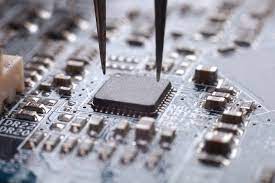
Inspection
Various methods are available to perform inspection with SMDs. In this study, we will look at two key methods for this purpose: Automatic optical inspection (AOI) and visual inspection (SPI). The former method is used to inspect the ICs after solder paste has been applied, while the latter method can be used to inspect the ICs before reflowing.
AOI utilizes a number of visible light sources such as LEDs, video cameras, and computerized systems to scan the solder joints. During this process, the light reflected from the components allows inspectors to determine the curvature of the solder joints. This information allows them to detect bad wetting, and missing components. However, this method is not suitable for detecting components that are covered with frames or borders.
The market for SMT inspection equipment is highly consolidated, with few large vendors controlling most of the market share. Key players are investing heavily in R&D, expanding their product portfolios, and acquiring other companies. Some of the major companies in this market include Micronics, Koh Young, and Test Research.
AOI is a popular technology for PCB inspection. It is faster than MVI and eliminates human error. Another major benefit of AOI is that it can quickly inspect components that are hidden under packaging or BGAs. As a result, AOI can help to ensure that a finished product meets specification.
MVI can be implemented in a variety of production environments and is cost-effective. It does not require expensive equipment. All you need is a magnification device and a staff that knows what to look for. The inspection staff should have access to design specifications, and should be trained to recognize defects and other problems.
Repair
When it comes to repair, there are a few different methods. The most common type of SM repair is done with hot air, but other methods can be used as well. One of the most advanced methods is laser rework.
Laser rework allows engineers to repair devices with extremely tight interpackage spacing. In addition, laser rework equipment allows for real-time thermal profiling, which is critical to effective rework. SM devices are electronic components that are attached to printed circuit boards.
The process of assembling SMD devices makes them small and fast. This convenience is specific to every Surface Mounted Device Company. SM devices come in many different shapes and sizes, and are commonly classified by electronic functions. In addition, SMD repairs are a good way to extend the life of your surface-mounted electronics.
Another method to repair SMDs is using an SMD reworking tool. These tools are designed to remove and repair a variety of surface-mounted devices. They come with a variety of advanced features, such as an auto-cooling feature that lowers the nozzle temperature after each use.
They also feature knob-style controls and a dual-line digital display. SM technology allows electronic components to be mounted directly onto the PCB surface, without the need for drilling. This method is more efficient and allows for a smaller number of drilled holes compared to through-hole technology which is totally different.
SM components are also more compact and suitable for higher routing density. The process for manufacturing surface mount devices can be very challenging and time-consuming, but is a great option for electronics technicians and manufacturers alike as it is affordable and easy to learn for most beginners in the industry.